

Welcome to the fascinating realm of photolithography, where precision meets innovation to sculpt the future of microfabrication. In this article, we’ll delve into the intricacies of photolithography, exploring its principles, applications, and the transformative impact it has on industries ranging from semiconductor manufacturing to biotechnology.
The Essence of Photolithography:
Photolithography, often referred to as “light printing,” is a cornerstone technology in the production of microelectronic devices. At its core, it involves using light to transfer a geometric pattern from a photomask to a light-sensitive chemical photoresist on a substrate. This intricate process lays the foundation for creating intricate patterns on the nanoscale, enabling the production of advanced integrated circuits and microdevices.
The Dance of Light and Precision:
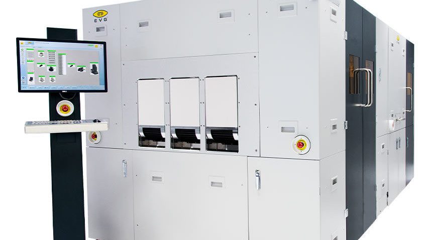
Central to the photolithography process is the photolithography machine, a marvel of engineering that orchestrates the delicate dance between light and precision. These machines utilize advanced optics, precise motion control systems, and cutting-edge exposure techniques to achieve unparalleled levels of accuracy. The result is the creation of intricate patterns with feature sizes that can reach the sub-micron and even nanometer scale.
Applications Across Industries:
Photolithography’s impact extends far beyond the realm of semiconductor manufacturing. Its applications span various industries, including:
Semiconductor Manufacturing:
The heart of the electronics industry, photolithography is indispensable for creating the intricate patterns on semiconductor wafers, laying the foundation for the production of microprocessors, memory devices, and other integrated circuits.
Biotechnology:
In the field of biotechnology, photolithography plays a pivotal role in creating microarrays, lab-on-a-chip devices, and other precision tools used in genomics, proteomics, and diagnostics.
MEMS (Micro-Electro-Mechanical Systems):
Photolithography enables the fabrication of tiny mechanical and electrical components that form the building blocks of MEMS devices, used in sensors, actuators, and other micro-scale systems.
Optoelectronics: For the production of devices like LEDs, photodetectors, and other optoelectronic components, photolithography is crucial in defining intricate patterns on light-sensitive materials.
Challenges and Innovations:
While photolithography has revolutionized microfabrication, it faces ongoing challenges, such as the push for smaller feature sizes and the need for alternative techniques to overcome diffraction limits. Researchers and engineers are continually pushing the boundaries of innovation, exploring new materials, techniques, and approaches to address these challenges and unlock new possibilities in precision microfabrication.
Conclusion:
In the ever-evolving landscape of technology, photolithography stands as a beacon of precision, enabling the creation of the microscale wonders that power our modern world. As researchers and engineers continue to refine and innovate, the future of photolithography holds the promise of even greater precision, unlocking new frontiers in electronics, biotechnology, and beyond. Stay tuned as we continue to explore the fascinating world of photolithography and its transformative impact on the way we build the future.
kingsmg-machinery